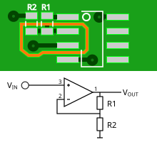
Driven guard
This article needs additional citations for verification. (October 2016) |


A driven shield is a method of electrical shielding used to protect low-current circuits against leakage current. A driven shield is often referred to as a driven guard, especially when applied to PCB traces.
Description
[edit]It is used in situations where the tiny leakage of current through the insulating surfaces of a wire or PCB board would otherwise cause error in the measurements or functionality of the device. The basic principle is to protect the sensing wire by surrounding it with a guard conductor that is held at the same voltage as the wire so that no current will flow into or from the wire. This is typically achieved using a voltage buffer/follower that matches the guard voltage to the sensing wire voltage, or in low-voltage differential sensing with an instrumentation amplifier, the common-mode voltage. The leakage from the shield to other circuit elements is of little concern as it is being sourced from a buffer which has a low output impedance.
The technique is used in equipment such as sensitive photomultiplier tubes, electrostatic sensors, precision low-current measurement, and some medical electrography machines, where leakage current would alter the measurement.[2] Any situation in which the source to be measured has a very high output impedance is vulnerable to leakage current and if sufficient insulation is not practical then a driven shield may be required. Coaxial cable is well suited for use as a guard; if electromagnetic shielding is also required then triaxial cable may be used as depending on the type of buffer circuit any noise on the guard may be amplified in the output.[3]
The limiting factor for this method is the input impedance of the voltage buffer, the JFET or CMOS op-amps typically used may have input impedances of many teraohms which is sufficient for most applications. Care must also be taken to ensure there are no unexpected paths by which leakage current may bypass the guard as this will defeat the system, and extra care must be taken in the design of the amplifier/buffer circuit to prevent oscillation as the guard, especially if it is used over a coaxial cable, may have a strong capacitive coupling to the sensing wire.
See also
[edit]References
[edit]
